This is the part two of my vaporizor writeup. You can find part one here.
Note: THIS POST IS INCOMPLETE
This post will go in depth though the design process.
Very in depth, also as if it were almost a tutorial on design and KiCad.
Please bear.
Power Supply
Now that I know the voltage and how much current it needs to be able to supply, I can start designing the power supply. Since it needs to output a whopping 6 watts, I decided to go with a switch mode power supply.
Types of Voltage Regulators.
Here, I'll discuss a few different types of voltage regulators.
First, there are the linear regulators. They are often quick and easy to use, but can be
very inefficient, espcially for high loads. That is because they act like a voltage divider,
but with feedback and stuff. It's advantages are that it gives a low output ripple and noise.
It's bad for this case because it is highly inefficient, and to make this project portable,
it is going to run off a battery. When a linear regulator is used to lower the voltage, all
that extra power goes directly to heat. For example, If there is a 12 volt input to a 5 volt
regulator, and the load pulls 1 amps, it will draw 1 amp from the 12V supply and dissipate
that as heat. So in this example, it would be something like 7 watts per amp drawn.
(12V - 5V) * 1A
On the other hand, switch mode power supplies tend to be more efficient. They work by switching the output on and off really quickly and smoothing out the ripple with inductors and capacitors, until you get the desired voltage. It is similar to how a PWM signal works to "fake" an analog signal with a digital signals. In fact, I will be using a PWM signal to a transistor to create a buck converter.
Buck converters are a type of switch mode power supplies when the output voltage is lower than that of the input. Boost converters are used to increase the voltage from a lower source.
The Microcontroller
I needed a microcontroller of some sorts to basically control the vaporizer. A simple operation would be that it has a button and the coil/power supply connected and would turn the power on when the button is pressed. I was going to use a buck converter, so the microcontroller should output the PWM. I did some quick search for cheap and small microcontrollers. I found and decided to use the ATTINY10 of the AVR microcontroller series. These things are tiny and consume very little power, also being perfect for small embedded projects like this.
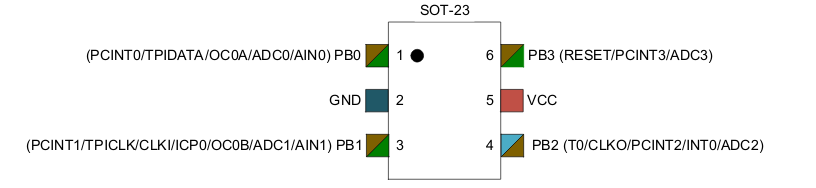
The above is the pinout diagram of the attiny10 microcontroller. There are two pins for power
(VCC and GND), and a whopping number of 4 GPIOs, which is more than enough. For the basic operation,
we only really need two I/Os, one for the button and another for the PWM output. The other two I/Os
can be reserved for extra functionality. I originally planned to have one for LED and the other
for voltage output feedback, to ensure that the voltage is actually what we want.
Looking at some other features of the attiny10, it's got a programmable timer, two PWM channels, 4 8-bit ADCs.
Designing a Buck Converter
A basic buck converter looks and works like this:
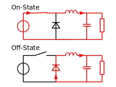
As mentioned above, the output voltage can be changed or set by changing the duty cycle of the
on/off times of the switch. The on-off signal from the switch is then 'smoothed' out via the
LC filter. At first, I was looking to use a built-in switching regulator, but most of them
seemed to need external inductors anyways. And since I'm already using a MCU for the PWM and to
do other stuff as well, I decided to just build a buck converter.
Texas Instruments had this document SLVA477B on designing the power stage of a buck converter, which was very useful. I just followed through the calculations to get the desired output.
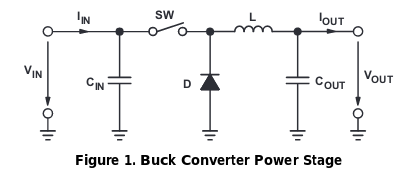
In my design, I replaced the switch with a transistor. I used an PFET instead of NFET since it
will be easier to drive it due to biasing (stackexchange).
To choose a transistor, I went on Digikey's parameteric search. I ended up with DMG2305UX.
The most important parameters in this case I think were the threshhold voltage and the voltage+current rating.
The current has to be higher than 2 amps. This one can deal with 4.2 amps, to be safe.
[TODO: Insert More Design Stuff and Calculations]
With that and following the TI SLVA477B document, I got roughly all the values I needed for the buck converter.
Schematics
Here's what my entire schematic came out to look like:
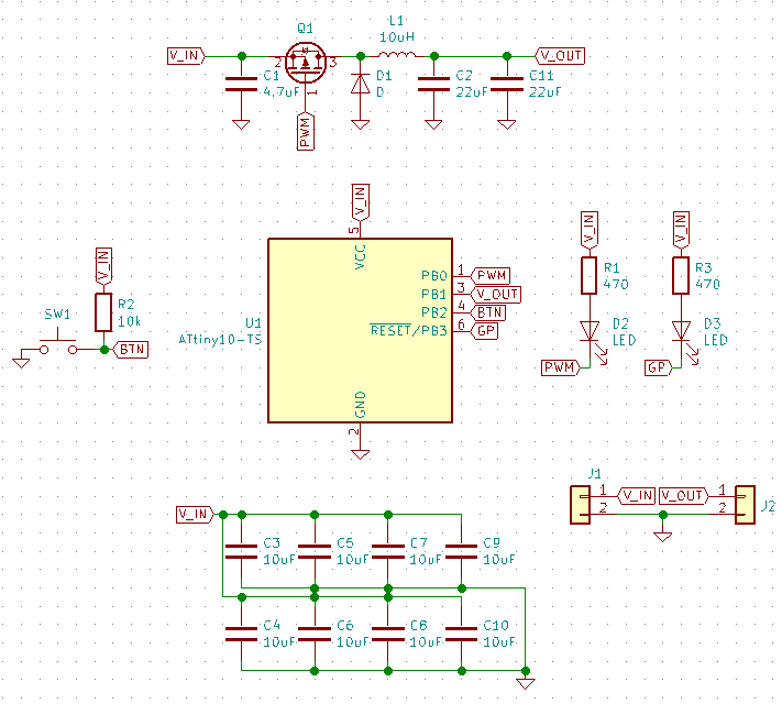
The top part is the buck converter and it is basically the circuit shown in the previous section.
I added another 22uF capacitor for more filtering and the microcontroller part is fairly
straightforward. The 10k resistor (R2) is there as a pull-up.
The PWM output pin actually also drives the indicator LED (D2) as well.
This works because the anode is held high so it will light when the output is driven low,
which is when the P-channel MOSFET is turned on.
This has a bonus effect of indicating the power output depending on the PWM duty cycle.
There are two other pins that are connected that I haven't discussed yet, but we'll come back to them later.
The capacitor back on the bottom is for decoupling. What that means in this case is that it "de-couples" the AC noise from the DC signal. When the device is triggered, it starts to output and the coil will consume about 6W of power, and that is no small amount (for a circuit like this). When something like that happens, voltage (or current) can't immediately start to flow and the V_IN voltage will drop. If that drops significantly, it may not be enough to power the microcontroller. So by having a capacitor bank, it allows the sudden changes to happen without dropping the input voltage (kinda like having a water tank and then suddenly everyone turns their faucet on at the same time).
I actually didn't populate all of these capacitors, but I had a few extra just in case.
With all that, it was time to do board layout.
Wait, wait... Just to really make sure before I went through all the troubles, I simulated the buck converter circuit in LTSpice. If I could just find the files somewhere...
Simulation
The only thing I was really unsure about was whether the transistor I picked out can handle
the load and also operate properly in the way I set it up.
Usually, the manufacturers provide models for their components for simulation... in some way.
I Googled for "DMG2305UX spice model" and there was one just on the first few hits. (link)
Then I followed the steps here to import that into LTSpice.
The following is the test circuit I drew up:
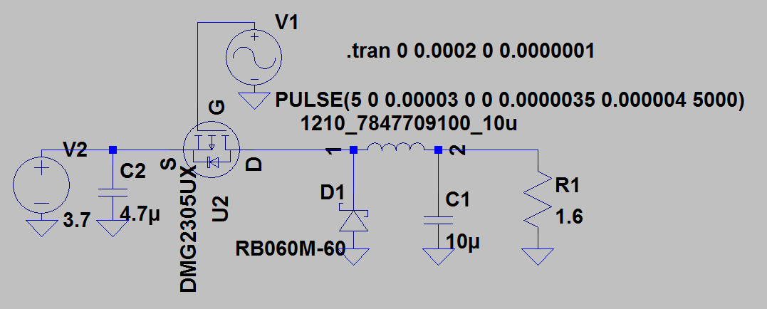
Here, V2 is the power source (the battery) and V1 is the PWM input to the gate of the transistor (U2).
The PWM signal is defined by the long PULSE(blah blah) text, each number corresponding to:
off voltage, on voltage, time delay, rise time, fall time, on time, period, and number of cycles.
In this case, the period is 4e-6 and on time is 3.5e-6 which is a duty cycle of 0.875.
The on and off voltages are reversed because a P-channel MOSFET will turn on "when the gate voltage is low."
From that we can roughly predict what our output voltage is going to be:
Input * (duty cycle) = output = 3.7V * (0.875) = 3.2375V
Note that I added R1 as the load with 1.6 ohms, which was the measured resistance of the coil. A citcuit like this won't work properly if there is no load. If you look at the datasheet for a switching power IC, there will be a minimum load.
Here's the simulated waveform:
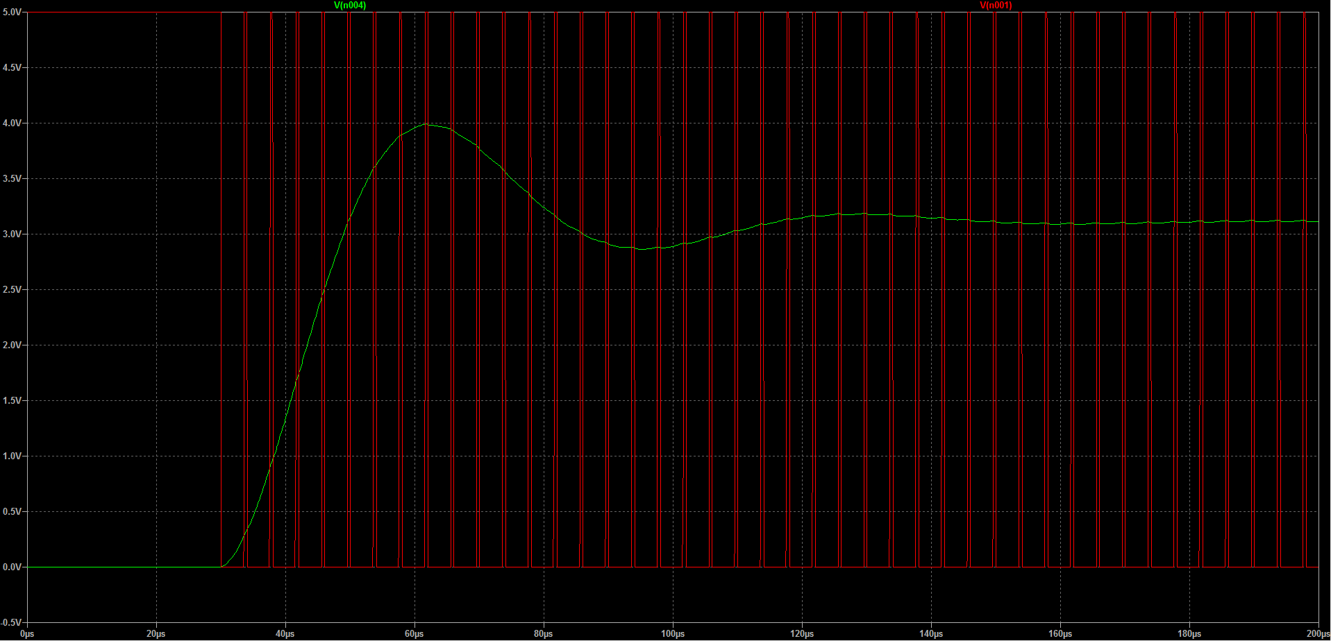
The red plots the PWM signal. Remember that I used a P-channel MOSFET, so it conducts on the low.
The green is the output voltage across the load R1. It rises once the PWM starts and eventually goes to the desired voltage, which seems to be around 3.2V looking at the figure.
The simulation files will be available is the GitHub repo as well.
Now that I have somewhat verified that this circuit will work, it was time for PCB layout.
(I also built the circuit to test it, but it is normally a good idea to simulate)
PCB Layout
Beware next block of text up to the layout diagram.
It's helpful info/tip for people new to this, but will bore you if you're familiar with the process.
If you don't like it, you may skip to the PCB diagram.
First thing you do after drawing out the schematic would be to annotate and perform a DRC.
In KiCad, the toolbar has a list of tools in order to move onto the PCB layout step.

The first automaticaly annotates all the components, the second (ladybug) runs electrical rules check. It will check for unconnected pins are floating nets and such. Although sometimes, there will be some you can ignore because of how the component pins are defined. For example, when you have header pins supplying power, it will warn you that there is no power input. That can be fixed by going to the options and marking that connection to connection type to be valid.
The third associates each component with a footprint. Some parts will already have one assigned, like the ATTINY10 I picked out when I selected the component to put on the schematic.
Anyways, I'll have to go through each and select a footprint for it for the layout.
After that, I can select the NET button to generate a netlist.
The next two are optional if I wanted to create a Bill of Matrials, listing all the components and the part number. The last button there moves over to the layout program.
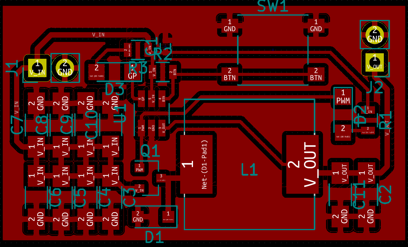
That's the layout I've come up with. I tried to make the entire thing as small as possible.
I planned on etching this myself, so I tried to fit everything on a single side as I'm not
yet ready to do double sided boards, with the lining up and vias and all that.
I think this is enough for the design. I'm gonna end it here. Might take for a bit for me to write about prototyping.
Thanks for reading.
73,
-Brian